IT之家 · 智能时代 · 10/12/2026, 22:45:30
Microsoft Unveils Maia 300 AI Chip: TSMC N2P Process, 288GB HBM4 Memory, and 18TB/s Bandwidth
Microsoft officially launched its third-generation custom AI chip, the Maia 300, featuring a multi-chiplet design on TSMC's N2P 2nm process. With 288GB of HBM4 memory delivering 18TB/s bandwidth and 13.8 PFLOPS FP4 compute power, it is scheduled for deployment in 2027 to support large-scale AI inference clusters.
SOURCE COVERAGEFull Original Report
On October 12, Microsoft officially unveiled the Maia 300 AI chip. This product features 288GB of HBM4 memory with a bandwidth of 18TB/s and delivers up to 13.8 PFLOPS of FP4 compute performance. Manufactured on TSMC’s N2P process node, it is scheduled for deployment in 2027.
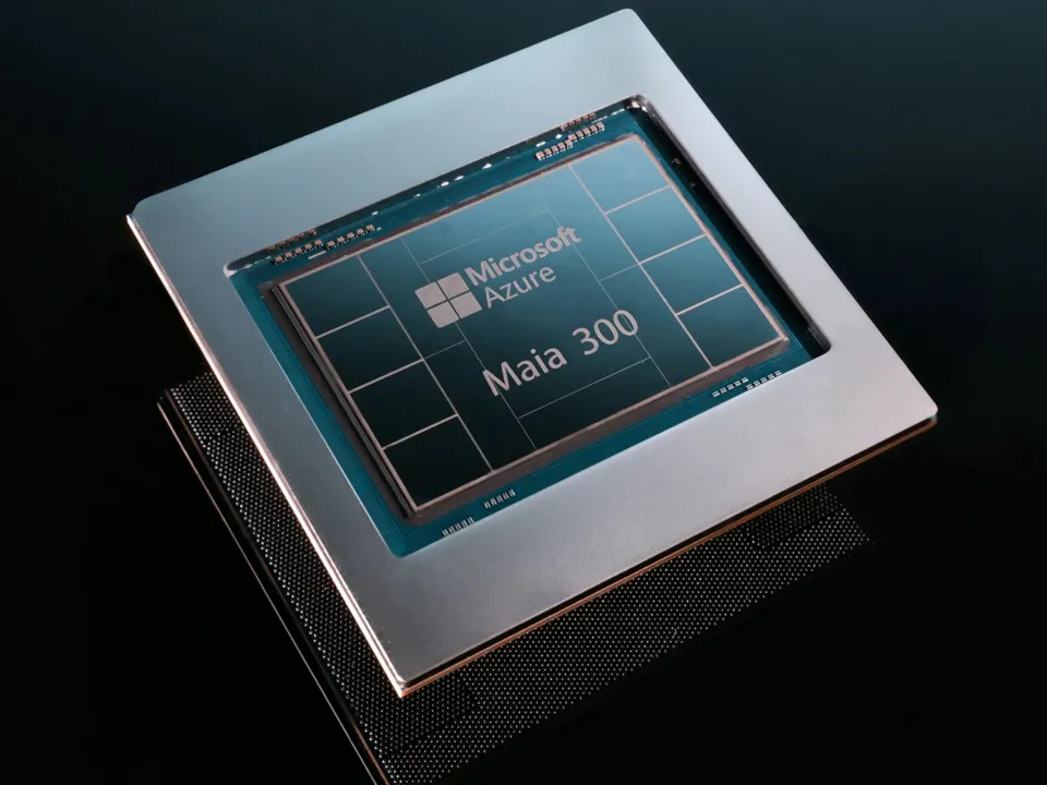
IT Home noted that the Maia 300 adopts a multi-chiplet design, with its primary compute die manufactured on TSMC’s N2P 2nm process, integrating separate memory and I/O chiplets. FP4 compute performance reaches up to 13.8 PFLOPS, while FP8 performance stands at 6.9 PFLOPS. The SoC has a rated power consumption of 950W, significantly higher than the 750W of the Maia 200.
Additionally, the product is equipped with eight stacks of HBM4 memory, providing a total capacity of 288GB and a bandwidth of 18TB/s, making it well-suited for AI inference tasks with high memory demands. Bidirectional scale-up interconnect bandwidth reaches 3.2TB/s, utilizing an Ethernet-based two-tier network architecture. A single rack can house 96 Maia 300 chips, enabling clusters of up to 12,000 accelerators.