IT之家 · IT业界 · 10/22/2026, 09:31:36
Micron Abandons 4F² DRAM for 3D Architecture and High NA EUV
Micron announced that 4F² DRAM lacks a viable scaling path due to cost and complexity issues, pivoting instead to 3D DRAM. The company's 8th-generation node (1ε) will introduce wafer bonding, while the first sub-10nm node (ζÅ) plans to adopt High NA EUV lithography, aiming for significant performance gains through 3D-stacked CMOS logic circuits.
SOURCE COVERAGEFull Original Report
On October 22, Micron held its annual 2026 Technical Webinar yesterday (local time), providing an outlook on DRAM, broad HBM, NAND, and SSD technologies. This article focuses specifically on foundational DRAM technology.
After more than two decades of technological exploration, Micron has concluded that 4F² DRAM lacks a viable path to scale due to complexity and cost constraints. With traditional 2D 6F² DRAM facing scaling bottlenecks, Micron has chosen 3D DRAM as its future development path.
IT Home noted that CXMT previously stated plans to launch 4F² hybrid bonding DDR5 RDIMMs within the year, while reports suggest Samsung Electronics abandoned the 4F² route for its first-generation sub-10nm class DRAM.
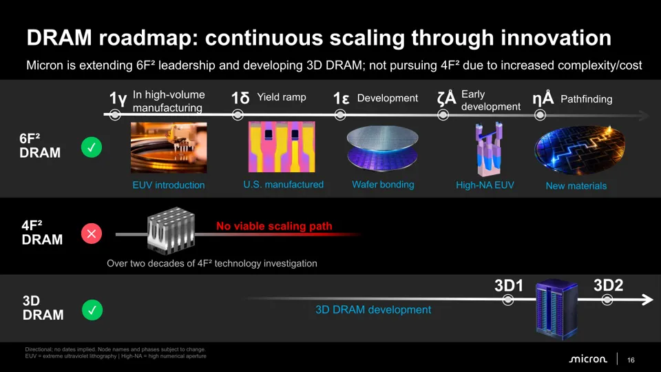
Micron’s 7th generation 10nm-class DRAM node, 1δ, is currently in the yield ramp-up phase. The 8th generation 10nm-class node, 1ε, introduces wafer bonding technology. The 1st generation sub-10nm-class node, ζÅ, is in early development and incorporates High NA EUV lithography. The 2nd generation sub-10nm-class node, ηÅ, is in the pathfinding stage with plans to apply new materials.
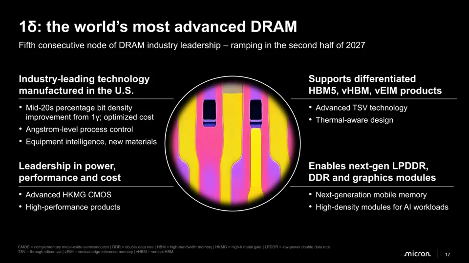
Micron stated that the 1δ process delivers approximately 25% generational improvement in storage density while maintaining optimized costs. This technology will be widely adopted across products such as HBM5, vHBM, vEIM, LPDDR, and DDR.
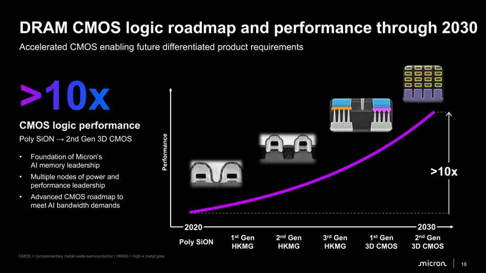
Micron indicated that DRAM CMOS logic circuits will also transition to 3D architectures, resulting in significant performance improvements.