Peking U and IBM Define Modern Analog Computing for Matrix Acceleration
Researchers from Peking University and IBM Zurich have published a review defining 'Modern Analog Computing,' shifting focus from differential equations to AI-centric matrix operations. Leveraging resistive memory (RRAM) for high precision and scalability, this framework aims to address energy bottlenecks in large models and establish new industry standards.
Full Report
Contents3 sections
What takes a GPU 100 iterations, this does in one step
By Cresci from QbitAI QbitAI | WeChat Official Account: QbitAI
Humanity’s two-thousand-year history of analog computing is being redefined.
In a Nature journal dedicated to unconventional computing, a review paper places "Modern Analog Computing" directly in its title, attempting to establish a formal definition for this field.
The work was led by Sun Zhong, a tenured associate professor at the Institute for Artificial Intelligence at Peking University. He also serves as the Chief Scientist of AnNex Chip, an analog computing chip startup.
Including Sun Zhong, the four authors hail from Peking University, IBM Research Zurich, and the Silicon Valley startup Unconventional AI—effectively gathering some of the most core forces currently driving the analog computing sector.

From left to right: Shahar Kvatinsky (IEEE Fellow), Sun Zhong, Abu Sebastian (IEEE Fellow), Piergiulio Mannocci
IBM has been deeply involved in analog and in-memory computing for over a decade, widely recognized as an industry benchmark. The review’s co-authors, Manuel Le Gallo and Abu Sebastian, are scholars at IBM Research Zurich; the latter is an IEEE Fellow and a long-term core researcher in this direction.
Meanwhile, Silicon Valley companies working on analog computing are being fiercely contested by capital. Unconventional AI’s valuation has exceeded $4.5 billion, while Normal Computing secured investments from Samsung and Eric Schmidt. Both companies claim they can "reduce AI energy consumption to one-thousandth."
Sun Zhong has consistently sought to unify this field. Two or three years ago, he did the same in the domain of in-memory computing, collaborating with international peers to publish a paper titled "A full spectrum of computing-in-memory technologies" in Nature Electronics.
He says the paper was merely an opportunity. His goal was to bring together several of the world’s most core institutions to jointly write the definition of "Modern Analog Computing."
How to Define "Modern Analog Computing"
In this review paper, refined over several years, the four authors position the word "Modern" as the pivot of their entire framework.
When mentioning analog computing, many people’s first reaction still lingers on the old machines that were replaced by digital chips half a century ago.
To clarify perceptions, the paper thoroughly distinguishes "Modern Analog Computing" from "Traditional Analog Computing" across three dimensions.
On the task dimension: Traditional analog computing focused solely on solving differential equations, whereas modern analog computing primarily targets the matrix computations that constitute the largest demand in the AI era and 6G communications.
On the hardware dimension: Traditional analog computing relied on CMOS analog circuits, while modern analog computing is rooted in new nanoscale devices such as Resistive Random Access Memory (RRAM) and other memristors.
On application feasibility: Traditional analog computing was constrained by low precision and poor scalability. Modern analog computing has explored engineering paths for high precision and scalability, using a rigorous system to clearly define boundaries, primitives, and evolution paths.

Understanding this new system requires re-evaluating the term "analog."
For many trained in modern engineering, digital computing represents "discrete," while analog computing is often assumed to correspond to "continuous."
In his presentation, Sun Zhong cited research by scholar Corey J. Maley, published in WIREs Cognitive Science in 2024.
The study points out that the core concept of "Analog" lies not in continuity, but in "Analogy"—mapping mathematical problems directly onto physical systems without binary symbolic abstraction, relying on natural physical laws to provide the answer.
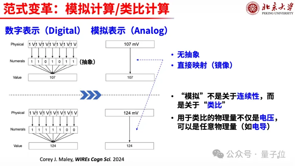
Everyday experience is actually full of shadows of analog computing.
When children learn arithmetic, one apple plus one apple equals two apples. To multiply 3×5, they group three piles of five apples together and count fifteen. This is the most direct physical mapping.
Analog computing chips perform the same analogy, seeking physical entities within microscopic circuits that correspond to mathematical variables.
However, doing so in traditional integrated circuits encounters obstacles.
The only physical quantities that change in real-time within a circuit are typically voltage and current. Once a resistor on a chip is manufactured, its resistance value is a fixed, unchangeable number.
If one tries to use Ohm’s Law to perform multiplication, both multiplicands are constantly changing. One number can be input as a voltage signal, but if the other becomes a fixed resistor, it cannot handle dynamic computational tasks.
The key to breaking this input limitation lies in finding a physical carrier for the circuit that can be rewritten at any time yet retain values for a long duration.
Resistive RAM (often referred to as memristors) provides exactly this possibility. The core characteristic of these new nanoscale devices is that their conductivity is not fixed; it can be precisely altered by applying electrical pulses, and the resistance value persists even after power loss.
This effectively opens up a new physical variable—"Conductance"—for integrated circuits beyond voltage and current, allowing for in-situ storage and adjustable regulation.
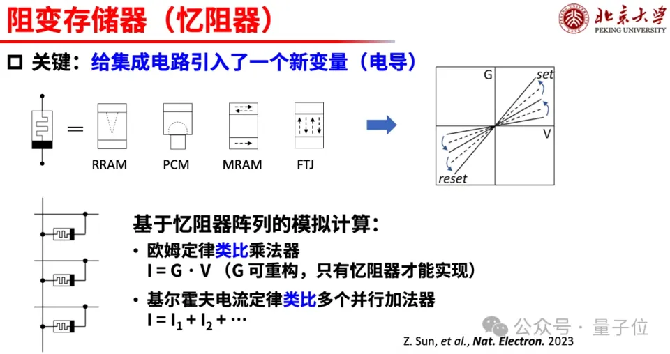
Thus, the two inputs for multiplication find their respective mapping anchors in the circuit: one number is directly programmed into the device’s conductance value, while the other is applied as voltage across the device terminals.
The moment current flows, according to Ohm’s Law, the magnitude of the output current is naturally the product of the two.
When voltages loaded on each row drive devices to generate multiple currents that converge into the same column wire, physical laws take over the computation again. According to Kirchhoff’s Current Law, the total current flowing into a node must equal the sum of the branch currents; parallel currents naturally aggregate and add up.
This means that single multiplications rely on Ohm’s Law, and multi-path summations rely on Kirchhoff’s Laws. The entire column’s multiply-accumulate results are computed all at once in the instant the wires converge.
By constructing closed-loop feedback paths with peripheral operational amplifiers, modern analog computing chips can further achieve equation solving.
Under the mechanism of negative feedback, the circuit spontaneously converges to a physical equilibrium state within nanoseconds upon powering on. The stable voltage at that equilibrium point is mathematically the solution to the equation.
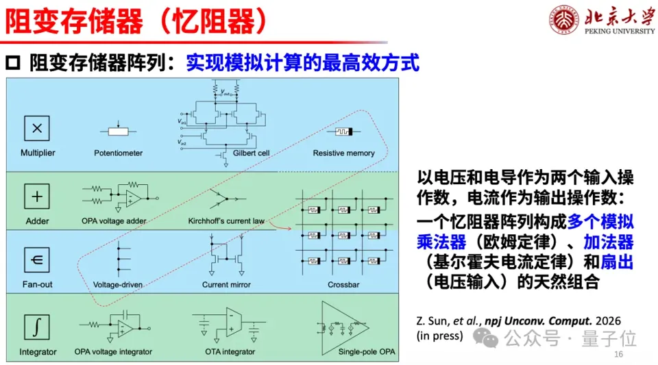
Beyond the constraints of physical variables, traditional analog computing faces another fatal bottleneck: scalability. It simply cannot scale up.
In the past, solutions based on CMOS operational amplifier circuits required stacking a large number of transistors for each operator, resulting in extremely poor area efficiency.
A 65-nanometer CMOS analog chip published in 2016 in JSSC, a top-tier integrated circuit journal, occupied a significant area yet could only accommodate four integrators and eight multipliers.
Moreover, analog voltage signals suffer from severe attenuation during long-distance transmission within circuits. Given that the footprint of CMOS operational amplifiers remains prohibitively high, integrating one million CMOS multipliers onto a single chip is virtually physically impossible.
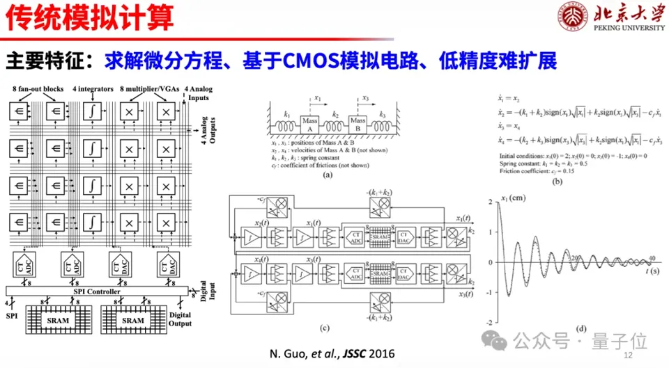
Novel memory devices have broken through this barrier. In a 1000×1000 crossbar array of miniature resistive random-access memories (RRAM), one million natural multipliers can now be compactly integrated at high density.
The reason modern analog computing has achieved a breakthrough in scalability lies in replacing complex CMOS analog units with novel resistive memory.
Resistive switching devices are essentially two-terminal nanoscale components, with dimensions of only tens of nanometers. In physical manufacturing, engineers need only lay out 1,000 horizontal metal row lines and vertically span 1,000 metal column lines across them. At every microscopic intersection where rows and columns meet, a layer of resistive material is inserted.
This three-dimensional network of 1,000 horizontal and 1,000 vertical wires directly interweaves to form exactly one million physical junctions within an extremely small chip area.
Each junction possesses an independent conductance value. When voltage is applied to the row line, current flows out at the junction. These one million nano-junctions naturally function as one million parallel in-situ analog multipliers.
Building upon this hardware evolution, this review paper categorizes analog computing into three core primitives: solving differential equations, solving matrix equations, and matrix-vector multiplication (MVM).
These three share a fundamental set of operators—adders, multipliers, and integrators—while being tightly coupled at both the mathematical and circuit levels.
Discretized differential equations can be transformed into matrix equations. Matrix equations can either be approximated iteratively via multiple matrix multiplications or solved directly in a single step using an analog closed-loop network. The mutual connectivity of these three forms constitutes a unified computational spectrum.
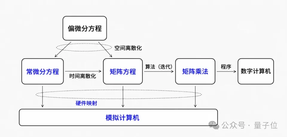
Sun Zhong stated that merely using analog circuits in isolation to solve a specific equation or perform multiplication holds little novelty. His original intention in writing this paper was to connect these scattered technical points, establishing a complete system for modern analog computing and defining a clear direction.
What Takes a GPU 100 Iterations, This Does in One Step
Defining a new system requires disruptive empirical data as support.
Currently, many teams in the integrated circuit industry are developing compute-in-memory chips, but the vast majority focus on the "matrix multiplication acceleration" route, primarily used for AI inference.
Sun Zhong and AnNaiZhiXin chose a path that is more technically challenging and distinctively differentiated: starting with solving matrix equations and matrix inversion.
Behind this choice lies the biggest pain point of digital chips in the real-world computing landscape.
In the heavy workloads of intelligent computing centers and scientific computing, over 80% of computational overhead is often spent on solving linear systems of equations in the form .
Mathematically, the core of solving this equation is calculating the unknown vector , which makes it difficult to bypass the hard hurdle of "matrix inversion."
Matrix inversion is precisely the operation that traditional digital chips fear most.
Compared to relatively simple matrix multiplication, the computational complexity of matrix inversion is extremely high, typically reaching .
Digital chips lack dedicated hardware units capable of performing direct matrix inversion. To complete a single inversion, general-purpose GPUs must rely on numerical algorithms, decomposing the task into dozens or even hundreds of matrix multiplications that require repeated looping and progressive approximation.
This directly results in massive amounts of expensive computing power and time being consumed by lengthy iterative calculations and data movement.
The Analog Matrix Computing (AMC) circuit designed by AnNaiZhiXin changed the rules. The team introduced a global negative feedback loop around the periphery of the resistive memory array, allowing the circuit's transient response to directly correspond to the solution of the matrix equation.
Operations that originally required a GPU to execute hundreds of iterations can now output precise solutions via a single measurement by the AMC circuit. The latency for a single operation is less than 100 nanoseconds, and this physical response time is independent of the matrix dimension size.

However, no matter how fast the computation is, if it lacks accuracy, analog chips still cannot leave the laboratory. Accuracy has historically been the "Achilles' heel" hindering the practical application of analog computing.
When Sun Zhong’s team demonstrated one-step matrix equation solving in PNAS in 2019, they were constrained by fluctuations in analog devices, resulting in a relative error of approximately 3%. The hardware array scale was also limited to 3×3.
This longstanding technical challenge was not thoroughly conquered until October 2025.
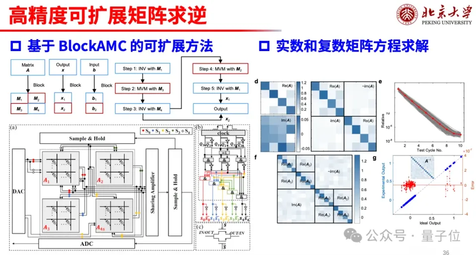
At that time, Sun Zhong’s team published a breakthrough paper in Nature Electronics, proposing a scheme for solving analog matrix equations that balances high precision with scalability.
Since continuous conductance states are prone to drift, leading to inaccurate calculations, the team borrowed the concept of Bit-slicing from early digital computers. They abandoned unreliable continuous states and instead adopted eight discrete conductance states per device (equivalent to 3 bits), which had been fully verified.

By concatenating eight 3-bit array slices, the system achieved 24-bit fixed-point precision.
Low-precision inversion determines the direction, while high-precision multiplication progressively eliminates residuals. After only three iterations, the relative error was reduced to , with subsequent convergence possible down to . This level of relative error matches the FP32 single-precision floating-point performance of digital processors.
Because bit-slicing supports depth expansion, this improvement in analog precision theoretically has no upper limit; it can be continuously enhanced by increasing the number of slices and iteration steps.
To address larger-scale real-world problems, the team designed a supporting BlockAMC blocking algorithm. This algorithm progressively decomposes massive matrices into sub-blocks that can be handled by the hardware array, completing inversion and multiplication in batches. Empirical tests have successfully extended this to complex matrices of 512×512 dimensions.
After solving the accuracy issue, the next immediate engineering challenge is how this analog system can seamlessly integrate with the existing digital world.
Sun Zhong and his R&D team are well aware that today’s IT infrastructure is built entirely on digital foundations. A purely analog chip isolated from the digital world has no commercial viability; analog computing must operate in synergy with the digital ecosystem.
In AnNexChip’s architecture, matrix operations are handled by dedicated micro-analog cores. The computed results are rapidly converted into digital signals via Analog-to-Digital Converters (ADCs). Data transmission between cores and across chips relies on digital channels, while non-linear operators such as square roots and trigonometric functions are processed by mature digital logic.
The team summarizes this collaborative approach as “Let matrices be analog, let logic be digital.”
When pursuing this hybrid analog-digital route, the most natural concern in the semiconductor industry often centers on interface overhead.
Each analog core requires Digital-to-Analog Conversion (DAC) before and ADC after its operation. Won’t the energy consumed by frequent conversions completely negate the power savings achieved by analog computing?
If one looks solely at the internal power distribution of the analog computing module, DACs and ADCs indeed account for the majority of consumption.
However, thanks to the bit-slicing architecture design, each sub-array only needs to process 3-bit data. The peripheral circuits do not require high-specification ADCs with over ten bits of resolution and high sampling rates; instead, basic converters with 6–8 bit resolution and a 10 MHz sampling rate suffice.
In chip design, relaxing precision and sampling rate specifications can significantly trade off for lower power consumption and smaller chip area.
Therefore, even when accounting for all front-end and back-end analog-digital conversion overheads, empirical evaluations show that under equivalent FP32 computational precision compared to digital chips, this analog matrix computing solution achieves throughput approximately 1,000 times that of a single NVIDIA H100 core or digital ASIC, and energy efficiency roughly 100 times higher than the latter.
Beyond superior compute metrics, this architecture also bypasses high-cost foundry barriers in manufacturing and supply chain.
Digital GPUs must continuously invest in extreme ultraviolet (EUV) lithography advanced nodes like 3nm and 2nm to increase compute density. In contrast, resistive random-access memory (RRAM) devices can be reliably manufactured using mature 28nm or even 22nm processes.
Domestic wafer foundries have accumulated expertise in mature RRAM device processes comparable to international giants, enabling chips to be produced with autonomous and controllable capacity. This results in a comprehensive cost advantage of approximately 10x compared to mainstream GPUs.
With a foundation offering 1,000x throughput, 100x energy efficiency, and 1/10th the cost, the commercialization of this technology directly targets real-world scenarios where the industry has the most urgent need for solving linear equations and matrix inversion.
In the short term, AnNexChip expects to release an empirical demonstration within one year targeting embodied AI motion control and planning.
When robots perform high-dynamic motion control, they must solve complex dynamic matrix equations in real time. The microsecond-level solving capability of AMC circuits allows robot joint movements to eliminate stuttering, becoming smoother and more fluid.
In the medium term, AnNexChip focuses on large-scale MIMO signal processing in 6G wireless communications.
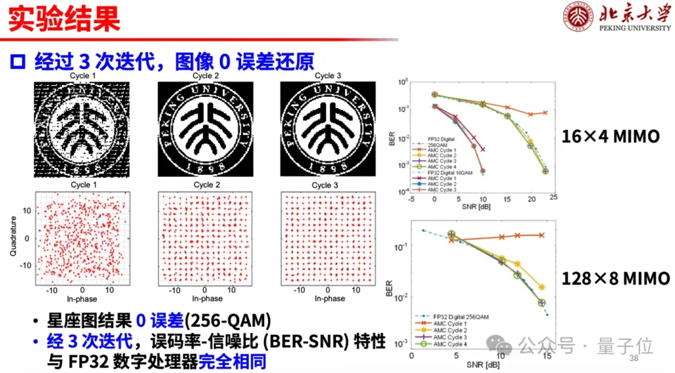
The underlying logic of wireless signal detection is also solving channel matrix equations. In large-scale MIMO experiments for 5G-A and 6G base stations, the Peking University team has already achieved zero-error reconstruction of the PKU emblem image and 256-QAM constellation diagrams after just three iterations. Their Bit Error Rate (BER) curves overlap with those of digital FP32 solutions.
In longer-term plans spanning 3 to 5 years, the team aims to scale the chip to thousands of parallel analog cores, natively supporting second-order optimization training for Large Language Models (LLMs).
Second-order optimization theoretically converges faster than traditional first-order methods but requires solving the inverse of the Hessian matrix at every step. Past digital GPUs were incapable of handling this, forcing model developers to settle for approximations using five iterative matrix multiplications.
Once native hardware-supported high-precision analog matrix inversion is deployed, the physical bottlenecks in LLM training optimization will be alleviated.
This Time, Silicon Valley and China Define It Together
In the fields of semiconductors and frontier computing, people have long been accustomed to a fixed script: Silicon Valley pioneers a new technical path, and domestic teams quickly follow suit.
But on the track of modern analog computing, the narrative has reversed.
It was Chinese scholar Sun Zhong who led the joint effort with IBM Research Zurich and Silicon Valley unicorns to define the direction and set the boundaries for the entire field.
On this front, the seminal paper came from his team, and he broke through the accuracy bottleneck that had plagued the industry for decades.
Meanwhile, on the industrial side, two Silicon Valley unconventional computing star companies valued at billions of dollars are following core paths extended from his research.
Securing the "dealer" position in this field representing the future of frontier computing relies on hardcore strength in two dimensions.
Academically, in 2019, Sun Zhong published research on solving matrix equations in one step using resistive arrays as first author in PNAS. This was the foundational paper for this direction.
The 2025 Nature Electronics paper, which tackled the accuracy bottleneck, set the highest readership record for the journal since its inception nine years ago upon publication.
This achievement received in-depth coverage from mainstream media, was selected alongside DeepSeek as one of the “Top 10 Domestic Tech News Stories of 2025,” won the “Top 10 Advances in Chinese Chip Science 2025” and the “Industry Sprout Award,” was included in the permanent exhibition and Original Innovation Source Exhibition at the 2026 Zhongguancun Forum, and was rated as the “Best Academic Paper” at the 2026 China Computing Conference.
More persuasive than academic honors is the industrial pursuit from across the Pacific.
Two pioneering computing startups in Silicon Valley, heavily backed by top-tier capital, are evolving their technical foundations in sync with his research.
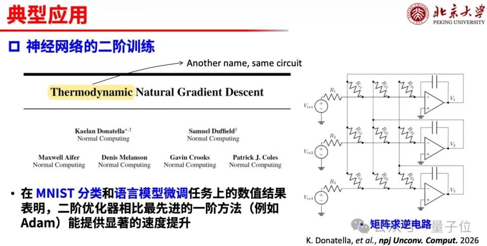
One is Normal Computing, founded by former Google Brain and Palantir teams. They taped out the thermodynamic computing chip CN101 in 2025 and have raised over $85 million cumulatively, with investors including Samsung, Eric Schmidt’s First Spark Ventures, and the UK’s Advanced Research and Invention Agency (ARIA).
In their 2026 paper “Thermodynamic Natural Gradient Descent” published in npj Unconventional Computing, along with subsequent second-order optimization work, the core solving hardware used is precisely the closed-loop negative feedback analog inversion circuit.
Sun Zhong clearly compared the topologies of both in his presentation slides, noting “Another name, same circuit,” demonstrating high consistency at the hardware level.
The other is Unconventional AI, founded by Naveen Rao, former Head of AI at Databricks, with a seed round valuation exceeding $4.5 billion.
Piergiulio Mannocci, a co-author of the review paper on “Modern Analog Computing,” previously collaborated closely with Sun Zhong at Politecnico di Milano and is now a key scientific researcher at Unconventional AI.
Sun Zhong noticed that the unconventional analog architecture philosophy advocated by the Unconventional AI team in their public talks aligned closely with his own academic perspectives, which he has been articulating for years.
It is worth exploring the mirrored differences in promotional narratives between companies in Silicon Valley and China.
Silicon Valley firms primarily highlight "reducing AI energy consumption to one-thousandth," a focus driven by the severe grid load bottlenecks they face.
In contrast, domestic teams like AnNaiZhiXin (Annazhixin) emphasize "increasing computing speed by 100 times." Given the objective constraints on computational resources, Chinese AI development faces more urgent demands for compressing model training and iteration cycles.
However, whether the goal is energy savings or speed improvements, both sides must ultimately cross the same critical threshold—precision—to move analog chips from the laboratory to industrial application.
As computer pioneer Richard Sutton revealed in The Bitter Lesson, the development of analog computing over the past half-century has also been marked by painful lessons.
Previous research often retreated to the limited value of low-precision hardware in fault-tolerant tasks. Yet, practical industrial deployments have repeatedly demonstrated that computing architectures lacking precision struggle to gain traction in mainstream industries.
Therefore, high precision is a prerequisite for new computing architectures to transition from the lab to industry. Following the publication of high-precision work in 2025, discussions within the international academic and industrial communities regarding "high-precision analog computing" have increased significantly, with the industry gradually converging toward this pragmatic standard.
After this review was published, "Modern Analog Computing" will enter the citation chain of subsequent research as a formal term. Its definitional framework originates from Peking University, endorsed by co-authorship from academia, industry, and research institutions across China and abroad.
For Sun Zhong, this is only the first step.
What he hopes to see more is that when this direction matures into an industry over the next five to ten years, looking back at the original defining literature, the signature page will bear the names of Chinese scholars.