Infineon to Build World's First 300mm GaN Power Semiconductor Fab
By IT之家Original title: 英飞凌将在欧洲建设全球首个 12 英寸氮化镓功率半导体大规模量产晶圆厂
68AI Score
Infineon announced plans to build the world's first 300mm (12-inch) fab for mass production of GaN power semiconductors in Austria, targeting operation by late 2027. The €1.1 billion investment aims to boost chip yield and process efficiency through larger wafer sizes, supported by approved EU state aid.
Full Report
IT之家 10 月 27 日消息,Infineon(英飞凌)当地时间今日宣布,将在欧洲建设全球首个用于生产氮化镓 (GaN) 功率半导体的 300mm(12 英寸)大规模量产晶圆厂。
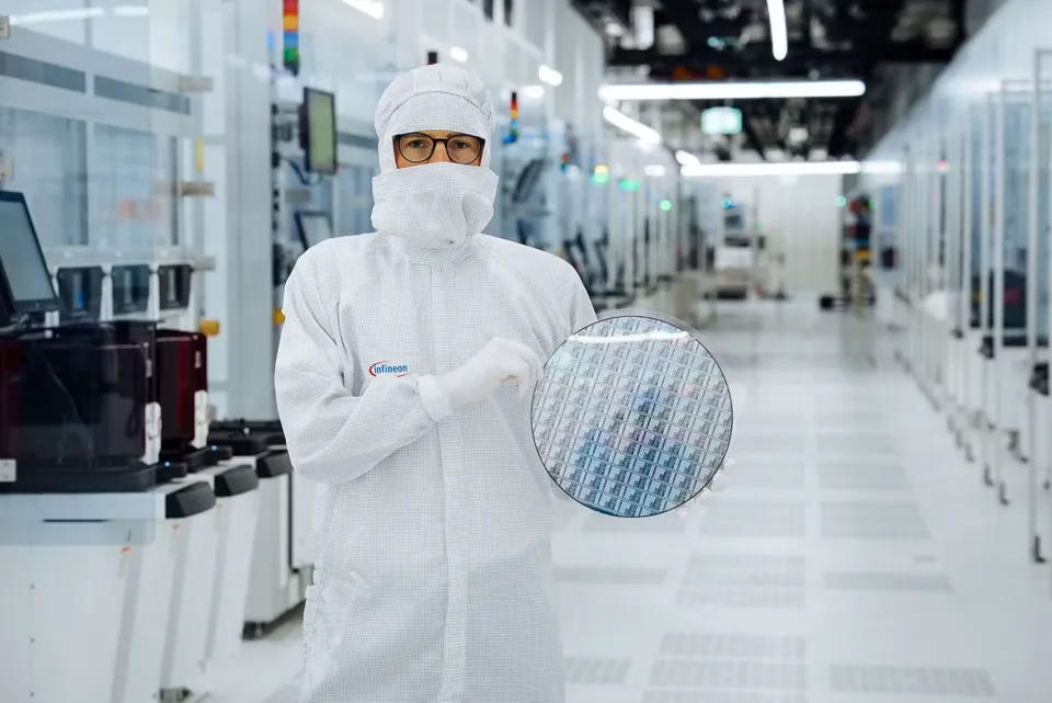
300mm(12 英寸)的单片晶圆芯片产出是 200mm(8 英寸)晶圆的 2.3 倍。更大面积的原料可助力生产工艺改进和效率提升。
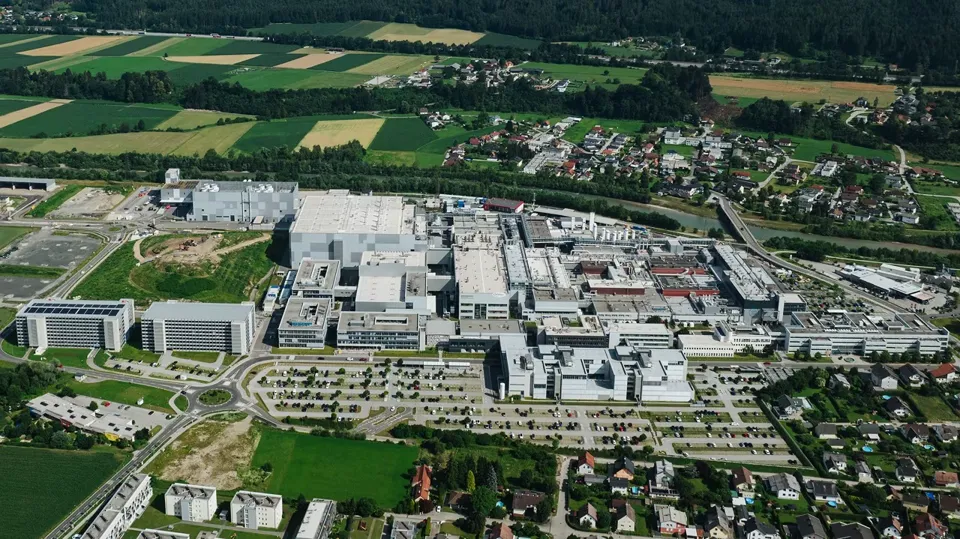
作为该计划的一部分,英飞凌计划在 2034 年前投资约 11 亿欧元(IT之家注:现汇率约合 82.19 亿元人民币),用于升级其位于奥地利 Villach 的现有洁净室设施。该工厂计划于 2027 年底投产。
欧盟委员会已批准向英飞凌的 Villach 扩产计划授予 3.19 亿欧元(现汇率约合 23.84 亿元人民币)的国家援助,奥地利经济部门预计将在规定的期限内正式履行这项资金承诺。