Qualcomm Validates HBC Tech; AI250 Chip to Sample in 2027
Qualcomm has completed hardware validation of its first-generation High Bandwidth Compute (HBC) technology, which stacks LPDDR memory for near-memory computing. The AI250 accelerator featuring HBC is scheduled to sample in early 2027, aiming to replace traditional HBM with a low-power solution delivering up to 133 TB/s effective memory bandwidth.
Full Report
IT Home reported on November 3 that Qualcomm announced yesterday the completion of hardware validation for its first-generation High Bandwidth Compute (HBC) technology at its San Diego, USA laboratory. The validation confirmed the technology's full read/write capabilities and near-memory computing functionality.
Qualcomm's HBC technology aims to boost AI inference memory bandwidth while reducing power consumption by stacking multiple layers of LPDDR memory directly above the compute chip.
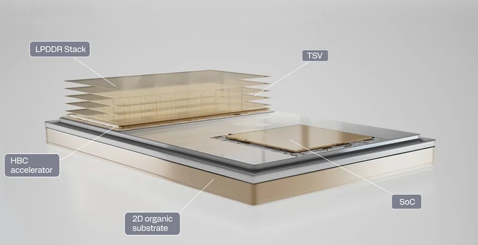
The AI250 accelerator featuring this architecture is scheduled to ship samples in the first half of 2027, signaling that this inference memory solution—replacing HBM with LPDDR—is entering the productization phase.

Note from IT Home: HBC (High Bandwidth Compute) is a near-memory computing architecture developed by Qualcomm specifically for AI inference scenarios. Unlike traditional HBM, which primarily increases bandwidth by stacking DRAM chips, HBC employs a vertical stack of multiple LPDDR memory layers interconnected via Through-Silicon Vias (TSVs). A compute chip is integrated at the bottom of the stack to handle near-memory processing, thereby reducing the data transfer distance between memory and processing units.
According to Qualcomm's previously disclosed technical specifications, HBC places compute units directly beneath the memory stack, shortening data transfer distances from several centimeters in traditional architectures to just a few micrometers. Qualcomm aims to leverage the relatively lower power consumption of LPDDR and the tight integration of compute and memory to improve data movement efficiency in AI inference workloads.
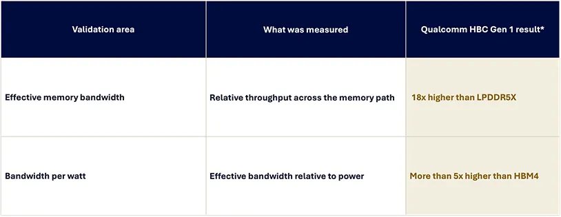
Qualcomm stated that the goal for HBC is to achieve bandwidth-per-watt performance six times that of traditional HBM solutions. Early samples used in this validation featured a two-layer DRAM stack. Test results showed bandwidth-per-watt exceeding five times that of HBM4, though it has not yet reached the previously announced target of six times. The final product is expected to utilize a four-layer stack design.
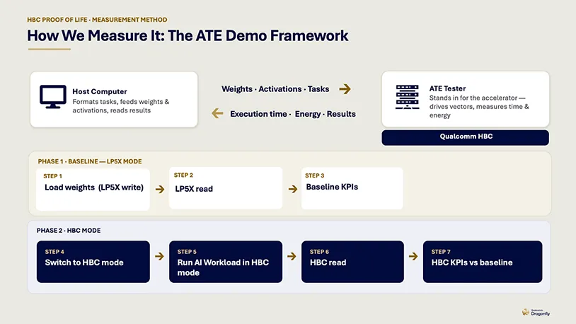
In terms of performance, Qualcomm announced that the first-generation HBC solution will provide the AI250 accelerator card with an effective memory bandwidth of 133 TB/s, representing an 18-fold increase over the AI200 accelerator card, which uses LPDDR5X memory.
Based on Qualcomm's data center product roadmap released in June 2026, the AI250 will feature first-generation HBC technology, while the subsequent AI300 is planned to adopt second-generation HBC. Qualcomm claims that the AI300's effective memory bandwidth design target will reach 54 times that of the AI200.