Tesla Updates AI Chip Roadmap, SI6 to Deliver 80x HW4 Compute
Tesla unveiled an updated AI accelerator roadmap: its sixth-generation inference chip SI6, built on a 2nm-class process with multi-chip module packaging, is projected to deliver 80x the compute of HW4, while the Dojo D3 training chip abandons the SRAM-centric wafer-scale design for a multi-die architecture with stacked HBM. Tesla also rebranded its accelerator line under the "Super Intelligence" (SI) naming.
Full Report
Contents3 sections
IT之家 November 8 news, Tesla has released an updated AI accelerator roadmap, further revealing the company's chip R&D direction for the coming years. According to this roadmap, the compute power of Tesla's sixth-generation inference accelerator is expected to reach 80 times that of the current fourth-generation chip; while Dojo D3, used for training tasks, will abandon its SRAM-centric architecture in favor of a multi-chiplet design equipped with stacked HBM high-bandwidth memory.
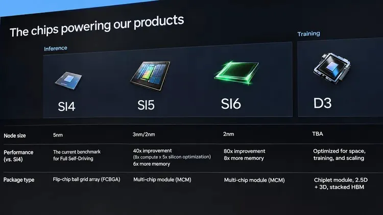
In addition, Tesla has also begun replacing the term "Artificial Intelligence" (AI) with "Super Intelligence" (SI), adopting the SI series naming for its AI accelerators. For the same reason, Musk recently also confirmed that SpaceXAI will be renamed SpaceXSI.
Tesla AI Accelerator Roadmap
According to the disclosed information, Tesla's current chip product line and plans are as follows:
| Item | HW3 / AI3 | SI4 / HW4 | SI5 / AI5 | SI6 / AI6 | Dojo D1 | Dojo D3 |
|---|---|---|---|---|---|---|
| Purpose | Inference | Inference | Inference | Inference | Training | Training |
| Process node | Samsung 14nm | Samsung 7nm | TSMC 3nm / Samsung 2nm | 2nm-class | TSMC 7nm | TBD |
| Architecture | Monolithic | Monolithic | Multi-chip module (MCM) | Multi-chip module (MCM) | Wafer-scale system (SoW) | Multi-chiplet |
| Packaging | FCBGA | FCBGA | MCM | MCM | InFO_SoW (training compute unit) | 2.5D + 3D |
| Memory type | LPDDR4 | GDDR6 | GDDR6 / GDDR7 (TBD) | GDDR7 (TBD) | On-chip SRAM | Stacked HBM |
| Memory capacity | 8GB | 16GB | 96GB | 144GB | 440MB SRAM per chip; 11GB SRAM per wafer | TBD |
| Memory bandwidth | ~68GB/s | ~224GB/s | TBD | TBD | ~10TB/s on-chip | TBD |
| Compute relative to SI4 | — | 1x | 40x | 80x | — | — |
| Estimated compute (TOPS) | 72 | 216–576 | 8640–23040 | 17280–46080 | 362 TFLOPS | TBD |
| Estimated compute (POPS) | 0.072 | 0.216–0.576 | 8.64–23.04 | 17.28–46.08 | 0.362 PFLOPS | TBD |
| Current status | Discontinued | Mass production | Near mass production | In development | Halted | In development |
Dojo D3: No Longer Adopting Wafer-Level Integration?
IT Home notes that the most noteworthy change in this roadmap may be Tesla's restart of its self-developed Dojo training accelerator project.
Musk canceled the entire wafer-level Dojo project in August 2025, and stated in August 2026 that SpaceX and xAI would fully adopt NVIDIA hardware in their ground and space data centers. However, the third-generation Dojo D3 will be significantly different from the first two generations, Dojo D1 and Dojo D2.
Tesla describes the next-generation Dojo D3 as a chiplet-based training accelerator that uses 2.5D and 3D packaging technologies and carries stacked HBM memory.
This is very different from the System-on-Wafer (SoW) architecture used by the original Dojo D1. D1 mainly relied on distributed on-chip SRAM and, through wafer-level packaging technology, connected 25 D1 processors to provide a total of 11GB of SRAM.
D3's shift to HBM means Tesla wants to significantly increase memory capacity. Modern AI models consume large amounts of memory to store model parameters, activations, and intermediate computation data. From a capacity perspective, SRAM is no longer suitable for meeting such demands.
Adopting HBM makes it easier to scale memory capacity, but it also introduces different trade-offs in latency, bandwidth, packaging, and power consumption. It is currently unclear whether Tesla has completely abandoned wafer-level integration technology.
One possibility is that Tesla will still use wafer-level packaging technology to connect logic chips and stack custom HBM modules on top of them.
Another possibility is that Tesla considers wafer-level integration too costly and valuable only in specific architectures dominated by SRAM. Continuing to stack HBM on logic chips that use wafer-level interconnects would further increase design complexity, thermal management difficulty, and manufacturing difficulty, potentially reducing chip yield while also creating long-term reliability issues and ultimately driving up costs.
Although most of these problems can be addressed by adding redundancy designs, improving process technology, and other means, such measures all increase costs. Therefore, it seems more likely that D3 will adopt a traditional chiplet architecture rather than wafer-level packaging.
At present, Tesla has not disclosed D3's specific compute performance, memory capacity, manufacturing process, or development timeline.
However, the company says Dojo D3 will be optimized for "space, training, and scalability." This means the product must not only provide sufficient computing performance but also have strong scalability. This further suggests that D3 may adopt a more traditional accelerator architecture rather than a wafer-level packaging solution.
More notably, D3 will also be optimized for deployment in space environments. This may mean that at least some models need to be radiation-hardened.
SI6: Compute Performance Expected to Reach 80 Times That of HW4 in the Coming Years
Another important piece of information in the roadmap is that Tesla disclosed the approximate compute level of the sixth-generation inference accelerator SI6: its compute performance is expected to reach 80 times that of HW4, and its memory capacity will be 9 times that of HW4.
The specific figures depend on how HW4's performance is measured. Based on current estimates, SI6's compute performance may reach 17,280–46,080 TOPS, or 17.28–46.08 POPS. However, it is still unclear which data formats SI6 supports, so these numbers remain uncertain and can only be used as a reference.
For comparison, NVIDIA's Rubin GPU has an inference compute performance of 50 NVFP4 PFLOPS, a training compute performance of 35 NVFP4 PFLOPS, and an FP8/FP6 compute performance of 17.5 PFLOPS.
It should be noted that NVIDIA Rubin has already begun shipping to customers, while Tesla SI6 is expected to launch only in 2029 to 2030.
Currently, the fourth-generation inference processor used in Tesla vehicles was originally called HW4, later renamed AI4, and most recently renamed SI4. This chip is manufactured by Samsung Foundry using a 7nm-class process and uses traditional flip-chip ball grid array (FCBGA) packaging, and is expected to carry 16GB of GDDR6 memory.
It should be pointed out that the relevant Tesla presentation reportedly contains an error, labeling the chip's process as 5nm-class when it should actually be 7nm-class.
Tesla describes SI4 as the performance baseline for current Full Self-Driving (FSD) technology, and future generations of chips will be measured against it. However, Tesla has not officially disclosed the chip's absolute compute performance, memory capacity, or power consumption, making accurate comparisons difficult.
Musk has said that HW4's performance is 3–8 times that of HW3. HW3's official compute performance is 72 TOPS, so based on this estimate, HW4's compute performance is approximately 216–576 TOPS.
According to the roadmap, the next-generation fifth-generation inference accelerator SI5 (also called HW5 or AI5) will adopt a multi-chip module (MCM) design, moving away from the traditional packaging used by HW4.
This chip will be manufactured using TSMC's 3nm and Samsung's 2nm-class process technologies, respectively.
Tesla expects SI5's compute performance to reach 40 times that of HW4. Musk previously explained that this improvement comes from two aspects: an 8x increase in computing capability, mainly thanks to more advanced process technology and more execution units; and silicon optimization bringing a further 5x performance improvement.
Based on this estimate, SI5's compute performance may reach 8,640–23,040 TOPS, depending on the actual performance baseline of HW4.
However, SI5's expected power consumption is also quite high, potentially reaching 250W–800W depending on the application scenario. Therefore, estimating its actual performance at this stage still involves significant uncertainty.
In terms of memory, SI5's capacity is expected to reach 6 times that of the previous generation, or 96GB. Depending on whether GDDR6 or GDDR7 memory is ultimately used, its bandwidth may range between 768GB/s and 1.536TB/s.
As for the sixth-generation inference accelerator SI6, Tesla plans to further increase its compute performance to 80 times that of HW4, with memory capacity reaching 9 times that of the current-generation chip.
Based on the above estimates, SI6's compute performance may reach 17.28–46.08 POPS, with a memory capacity of 144GB. For an AI inference accelerator, this means considerable scale in both compute and memory.
Tesla has signed an agreement with Samsung's foundry division, planning for the latter to produce its sixth-generation inference accelerator, with the cooperation lasting until 2033.
The latest roadmap shows that SI6 will use a 2nm-class process. Considering that the chip is expected to launch in 2029 to 2030, as well as Samsung's recently updated foundry roadmap, SI6 may use the automotive-grade SF2A, the performance-enhanced SF2P, or even SF2Z with backside power delivery technology.
Notably, Tesla does not appear to have plans to produce SI6 using Intel's 14A process at the Terafab facility in the 2030s.
On the packaging side, SI6 will continue the multi-chip module (MCM) design introduced with AI5/SI5/HW5. This choice is reasonable, as by that time Tesla will have accumulated R&D and production experience with its fifth-generation inference accelerator, while also keeping packaging costs within a relatively reasonable range.
Currently, many automakers are considering multi-chiplet designs and HBM memory for next-generation system-in-package (SiP) solutions, which will also drive up the manufacturing costs of the related chips.
As for when Tesla will introduce HBM into its inference accelerators, there is still no clear answer, but SI6 is likely not to adopt this type of memory yet.