Infineon Fabricates World's First 300mm SiC Power Device Wafer
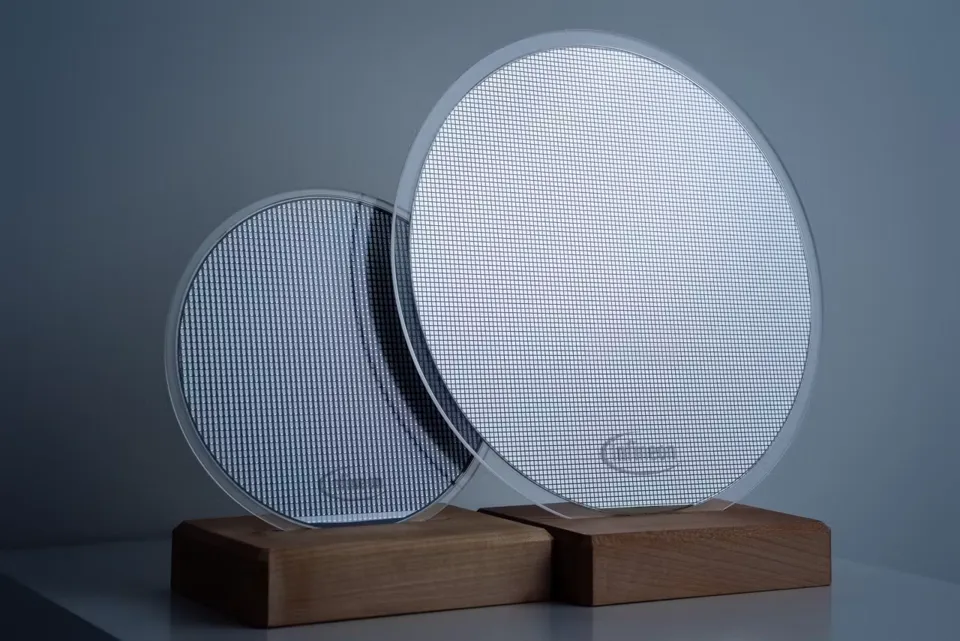
Infineon has become the first to process 300mm silicon carbide wafers into power semiconductor devices at full-scale production, using existing silicon equipment at its Villach fab in Austria. The company is advancing its 200mm SiC roadmap and has validated cold-split technology on 12-inch SiC at its Dresden site to cut ingot-to-wafer losses.
Related Entities
Full Report
IT之家 November 10 news, Infineon announced on the 9th local time that it has successfully taken the lead in processing 300mm (12-inch) silicon carbide (SiC) wafers into power semiconductor devices in a full-scale semiconductor fab environment.
This breakthrough is based on the existing silicon (Si) semiconductor manufacturing equipment at the Villach fab in Austria, demonstrating the practical commercial potential of large-size silicon carbide wafers. Infineon will work closely with customers and partners to plan the 12-inch SiC technology and mass production timeline, while further advancing its 200mm SiC manufacturing roadmap.
In addition, Infineon has also validated the feasibility of its cold split technology on 12-inch SiC at its Dresden fab in Germany. This process can improve the efficiency of the ingot-to-wafer process while reducing processing losses.